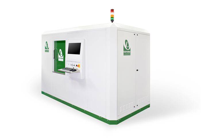
레이저 마이크로 머시닝 시스템
Laser Micro-machining Tool for Surface texturing & Thin-film patterning
Surface texturing |
Thin-film patterning |
Drilling |
Milling |
Cutting |
|---|---|---|---|---|
|
Friction reduction |
Flexible electronics |
Guide plate production |
Microfluidic devices |
Medical devices |
|
Biomimicry |
Display |
Calibrated holes for leak test |
Sample preparation |
Sensors |
|
Wetting |
OLEDs |
Fuel injectors |
Biomedical devices |
Wafer resizing |
|
Decorative |
Batteries |
Nozzles |
Micro moulds |
Stencils |
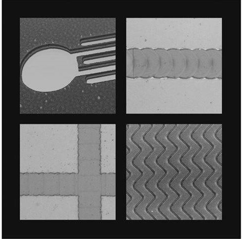
Surface texturing & Thin-film patterning
기판을 패터닝하는 데, 다양한 분야에서 레이저가 많은 인기를 얻고 있습니다. 얇은 층의 제거 또는 패터닝 또는 여러 층의 선택적 제거 시 기존 기술에 비해 많은 이점이 있습니다.
Laser patterning or thin film patterning can not only produce many intricate shapes, but selective ablation allows the removal of layers with thicknesses of less than 100 nanometres.
Particular interest is found in a number of applications from flexible electronics through to applications in the energy and medical sectors.
Dependent on the task at hand, Oxford Lasers have a wide variety of lasers available for laser patterning ranging from ultrafast picosecond and femtosecond lasers through to nanosecond and longer pulsed lasers. Dependent on the application, material and thickness of the layer(s) to be removed, different lasers are used to ensure fast high quality patterning.
Polymers
매우 높은 정밀도로 다양한 합성, 천연 고분자를 레이저 가공 할 수 있습니다.
Many polymers can be laser drilled and cut with extreme quality and precision, but care needs to be taken with the judicious choice of laser wavelength and pulse length to ensure best quality results. Laser drilled micro holes can be created as small as a few microns, whereas laser micro cutting can cost effectively produce features up to several centimetres and beyond.
To ensure the highest precision while processing both polymers and engineering plastics, the correct choice of processing conditions is extremely important to ensure that cumulative heat effects are avoided and high-quality results at the micron level are achieved. Often the colour of the polymer can significantly influence the choice of processing conditions.
Polymers as thin as a few tens of microns through to thicknesses of several millimetres can be drilled and cut.

A sample of polymers we can machine include:
ABS | Acrylics | Flouropolymers (PTFE/Teflon/FEP etc) | Polyimides (inc. Kapton) | Plus many more...
하나의 특정 그룹에 속하지 않거나 둘 이상의 재료 분류에 포함되지 않을 수 있는 다른 재료가 많이 있습니다.
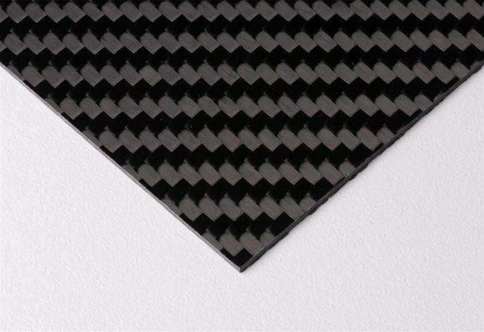
A sample of these include; Transparent Conductive Oxides (TCOs) such as Indium Tin Oxide (ITO) which is widely used as a thin conducting film due to its excellent electrical and optical properties. Composites such as carbon fibre, which have high tensile strength and low thermal expansion.
In addition, other common minerals such as Silicon Dioxide which is widely used in microelectronics.
A further class of materials is that composed of stacked layers, where the layers may vary from hundreds on nanometres through to hundreds of microns and beyond. Here lasers are particularly useful where top layers can be selectively removed without damaging the layers below e.g. in OLED stacks, metals on ceramics, metals on FR4 etc.
All of these materials and many others can be drilled, milled, cut or patterned with ultra-high precision producing features on the micron scale.
A sample of other material we can machine include:
Transparent Conductive Oxides (ITO, ZnO, SnO) | Composites (e.g. carbon fibre) | Silicon Dioxide (SiO2) | Plus many more...
Semiconductors
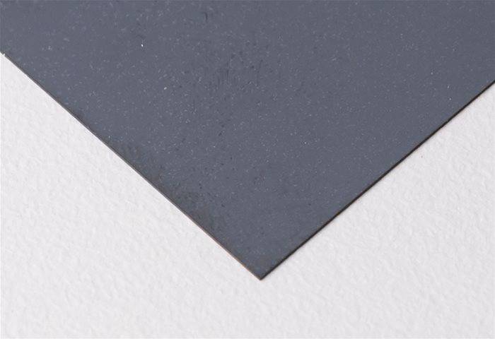
일반 도체 (conductor)와 절연체 (insulator) 사이에 전도율이 있는 이 재료 그룹은 고유 또는 외부 그룹을 형성하는 재료 클래스에 관계없이 매우 높은 정밀도로 레이저 가공 할 수 있습니다.
Laser micromachining can be used to process almost all semiconductors with ultra-high accuracy and precision. This can be particularly important as devices shrink in size where tolerances become ever more demanding. Lasers not only allow drilling of hard semiconductors like Silicon Carbide and Diamond, but also micro cutting where laser kerf widths are significantly reduced compared to conventional dicing or sawing.
Many semiconductor materials e.g. Silicon can not only be drilled and cut but can also be trimmed and the material wafers re-sized. Wafer resizing can routinely be achieved on wafers up to 300mm.
In addition, it is possible to mill or thin these semiconductor materials with degrees of precision approaching a few microns. This can be particularly useful for creating new devices or for semiconductor analysis.
A sample of semiconductors we can machine include:
Gallium Arsenide | Germanium | Silicon | Silicon Carbide | plus many more...
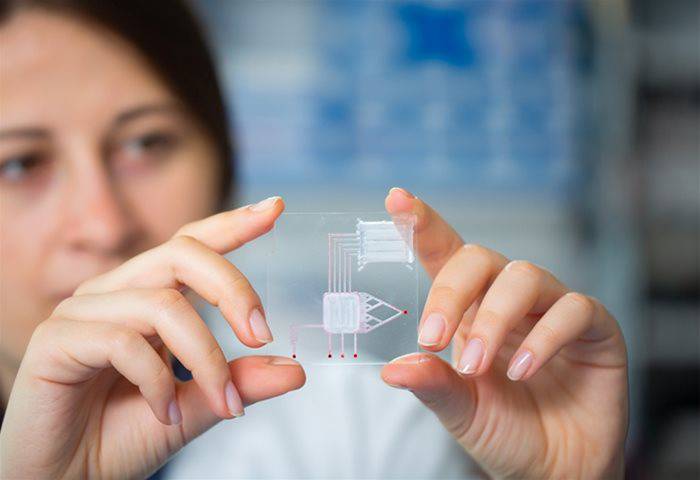
For Lab on a Chip Devices
Microfluidic device는 장치의 최종 목적에 따라 다양한 재료로 가공될 수 있습니다.
Often referred to as “Lab on a Chip” devices they can be used for a variety of processes including transport, separation, mixing or indeed act as reaction vessels. Such devices can be used in a variety of applications including cellular and bacterial processes, fuel cells, optofluidics, reaction chemistry etc.
Microfluidic devices typically have structures that are composed of channels and wells, which can be combined to act as micro pumps etc for fluid mixing. Channels have dimensions that are typically < 100 microns wide and 100 microns deep.
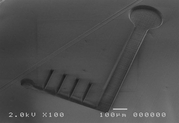
These devices can be made form a host of materials including glasses e.g. borosilicate, polymers e.g. PMMA etc.
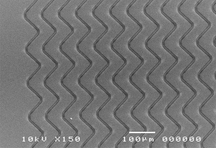
Direct laser ablation can produce a variety of shapes, see example images, of serpentine channels and wells which can be combined to produced complex structures. In addition, holes in the substrate can be created to allow the introduction of reagents.
For X-ray Microscopy
Nanoscale X-Ray Microscopy를 위한 Sample Preparation
반도체, 재료 연구 및 석유 및 가스 산업 전반적인 샘플 가공
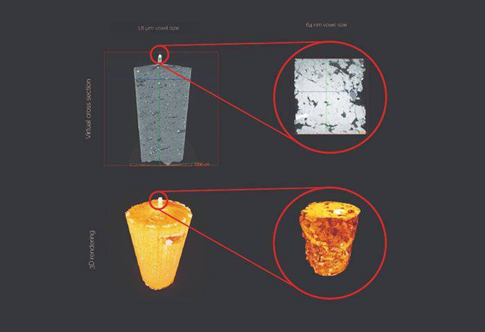
X-ray microscopy (XRM) provides three-dimensional imaging of internal micro and nanostructures across a range of specimen types and sample sizes.
High resolution 3D X-ray microscopes allows non-destructive imaging of samples for applications such as analysis of semiconductor devices, grain structures of metals in materials research and rock samples for the oil and gas exploration. Samples must be reduced in size to match the microscopes field of view and penetration depth and Oxford Lasers have developed a semi-automated sample preparation tool that efficiently performs this task.
Utilising a two-step laser process, a small sample is created from the bulk macroscopic material. Secondly, this sample is then reduced to an appropriate size for the application, typically 50 microns.
Sample preparation by laser micromachining is compatible with a range of materials from rock and ceramic, through to metals and semiconductors. Oxford Lasers have been producing and supplying sample preparation tools for over 10 years to companies and research institutes across the globe.
Milling applications
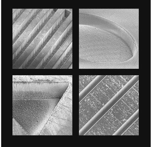
마이크로 밀링에 레이저를 사용하면 복잡한 많은 부품을 생산할 수 있습니다. 이 기술은 예를 들어 보이드와 채널을 생성하는 데 사용될 수있을 뿐만 아니라 피쳐를 둘러싼 재료를 제거하여 형성되는 융기된 피쳐를 생성 할 수 있습니다.
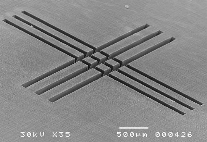
Laser milling allows the removal of material by typically scanning the beam across the surface of the substrate multiple times and often in multiple directions. This allows progressively more and more material to be removed while often preserving or improving the surface finish.
Milled features can have a variety of geometries from rectangular voids, through narrow channels, to raised features for example pyramids or pillars.
Oxford Lasers not only have a wide variety of lasers available to undertake micro milling, but crucially a variety of scanning modules and devices that allow us to produce almost any shaped feature.
Cutting applications
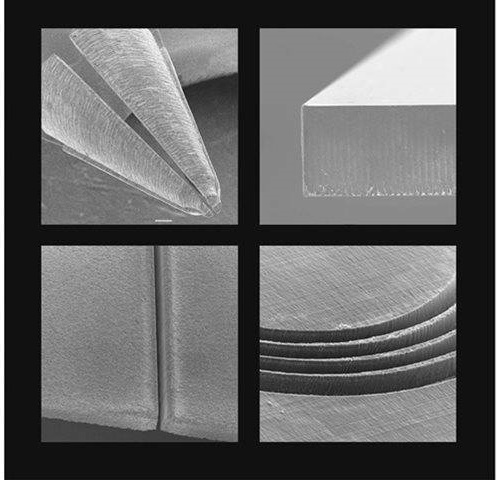
미세 절단을 위한 레이저의 사용은 다양한 산업에서 매우 인기가 있습니다. 초당 수 미터의 속도로 재료 표면을 가로 질러 레이저 빔을 가할 수 있는 능력은 탁월한 정밀도 뿐만 아니라 매우 신속한 절단을 할 수 있도록 합니다.
Laser cutting can not only produce linear cuts as common with traditional dicing or sawing techniques, but due to the ability to manipulate the beam in any direction, can produce any shape of cut in the original substrate material.
One unique benefit to the use of lasers when cutting, is the ability to produce extremely narrow kerf widths. This is important when either the material is expensive, or cuts need to be produced between pre-existing close pitched features.
Rather than cut completely through materials, it is possible to stop at a predetermined depth - this lends itself to a scribe and break process, which can not only serve to increase the speed of the cutting process, but also hold very small and delicate parts together before separation.
Oxford Laser have a wide variety of lasers available for laser cutting, ranging from ultrafast lasers which are particularly good for cutting transparent materials, to lasers with longer pulse lengths which can help to increase throughput.
Drilling applications
마이크로 드릴링을 위한 레이저의 사용은 전자 및 자동차 분야에서 디스플레이 및 에너지 분야에 이르기까지 다양한 산업 분야에서 널리 채택되고 있습니다.
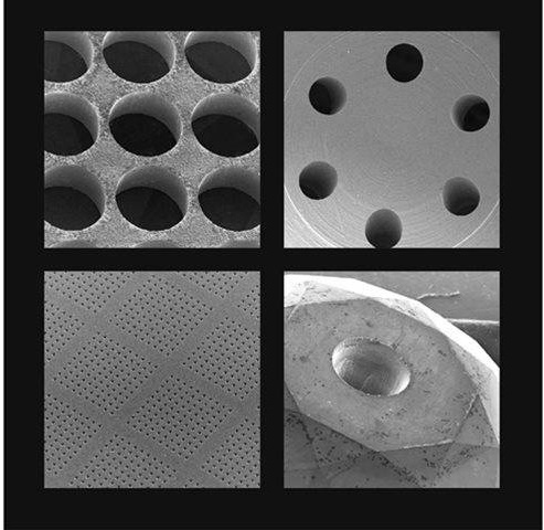
These applications can have a need, not only for a variety of hole geometries, but parts can have anything from a single hole to many tens of thousands of holes.
Laser drilling can produce not only circular and rectangular holes, but these holes can be produced with a variety of tapers. In addition, holes can be drilled at angles normal to the surface of the material or if required at very acute angles to the surface.
There are a variety of processing techniques available when undertaking laser drilling. These techniques can result in many hundreds of holes being drilled per second and / or these holes having extremely high quality, where hole after hole, the shape is identical.
Holes can be drilled on parts, where the hole positional accuracy is less than 2 microns.
Oxford Laser have a wide variety of lasers available for laser drilling. These range from ultrafast picosecond and femtosecond lasers through to nanosecond and longer pulsed lasers. This allows us to select not only the best laser pulse length, but also wavelength to suit your particular application.
Oxford Lasers have been laser drilling holes in a wide variety of materials for over 20 years.
