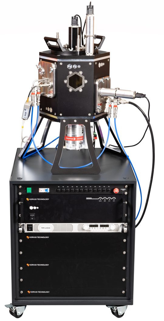
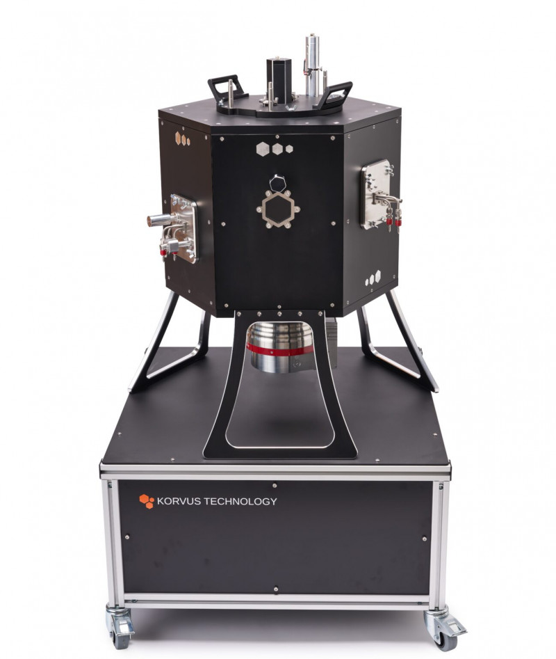
The HEX Series
Modular PVD Systems
HEX 시리즈는 독창적인 모듈식 아키텍처를 갖춘 벤치탑 장비로서, 박막 증착 분야에 비교할 수 없는 수준의 사용자 제어와 커스터마이즈, 업그레이드가 가능합니다.
HEX 플랫폼은 최신 박막 기술과 성능을 도입한 벤치탑 PVD 시스템입니다.
기존 PVD 챔버와 달리 HEX의 오픈 프레임 아키텍처를 통해 사용자가 기기를 자유롭게 재구성하거나 업그레이드할 수 있으며, 다양한 옵션의 추가가 가능합니다. 따라서 증착 연구 시 어떤 방향으로 진행되더라도 본 시스템을 통해 원하는 목표를 달성할 수 있습니다.
Concept
컴팩트하고 매우 유연한 박막 증착 시스템.
Design
HEX 시리즈 디자인의 모듈식 특성은 전문적인 도구가 없어도 패널을 몇 분 만에 프레임에 장착할 수 있음을 의미합니다.
Trusted by 100+ world-class brands and organisations of all sizes
Thin Film Deposition Systems
THE HEX SERIES
The HEX Series includes the benchtop HEX and the larger HEX-L and HEX-XL Systems
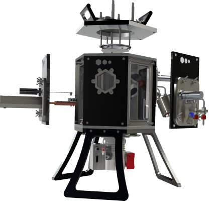
HEX
Benchtop or rack-mounted compact system

-
4″ (100mm) Maximum Sample Size Diameter
-
Up to 3 Deposition Sources
-
Magnetron Sputter Size (Diameter): 2"
-
12 L Chamber Volume (24 L When Stacked)
-
5×10⁻⁷ Base Pressure (mbar)
HEX-L
Larger mobile base-stand-mounted system

-
6″ (150mm) Maximum Sample Size Diameter
-
Up to 6 Deposition Sources
-
Magnetron Sputter Size (Diameter): 2" or 3"
-
50 L Chamber Volume (100 L When Stacked)
-
5×10⁻⁷ Base Pressure (mbar)
HEX-XL
Larger mobile base-stand-mounted system
-
12″ (300mm) Maximum Sample Size Diameter
-
Up to 6 Deposition Sources
-
Magnetron Sputter Size (Diameter): 3" or 4"
-
86 L Chamber Volume (172 L When Stacked)
-
5×10⁻⁷ Base Pressure (mbar)
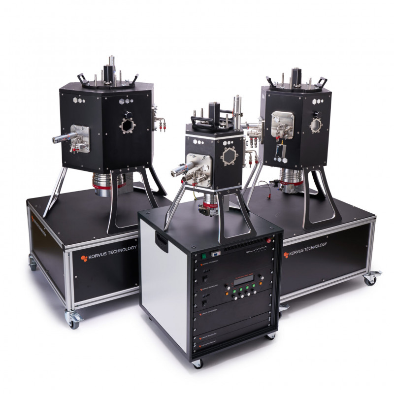
Highly Modular PVD Systems
Thin Film Deposition Systems
The HEX Series of thin film deposition systems are uniquely designed to be completely modular.
Each thin film deposition system comes with detachable side panels. This allows users to begin with a relatively simple setup and upgrade or reconfigure their system in-line with their research needs or budget.
These upgrades are modular and simple to install, eliminating system downtime.
The HEX Series includes the benchtop HEX and the larger HEX-L and HEX-XL Systems. (See “HEX vs HEX-L vs HEX-XL” page).
Modular Design for Rapid Re-Configuration
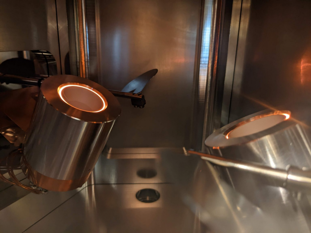
HEX 시스템은 가벼우면서도 대부분의 물리적 증착 응용 분야에 충분히 견고한 6면의 알루미늄 프레임을 갖는 고진공 챔버로 구성됩니다. 육각형 구조는 다음을 포함하여 6개의 모듈식 패널을 지원합니다.
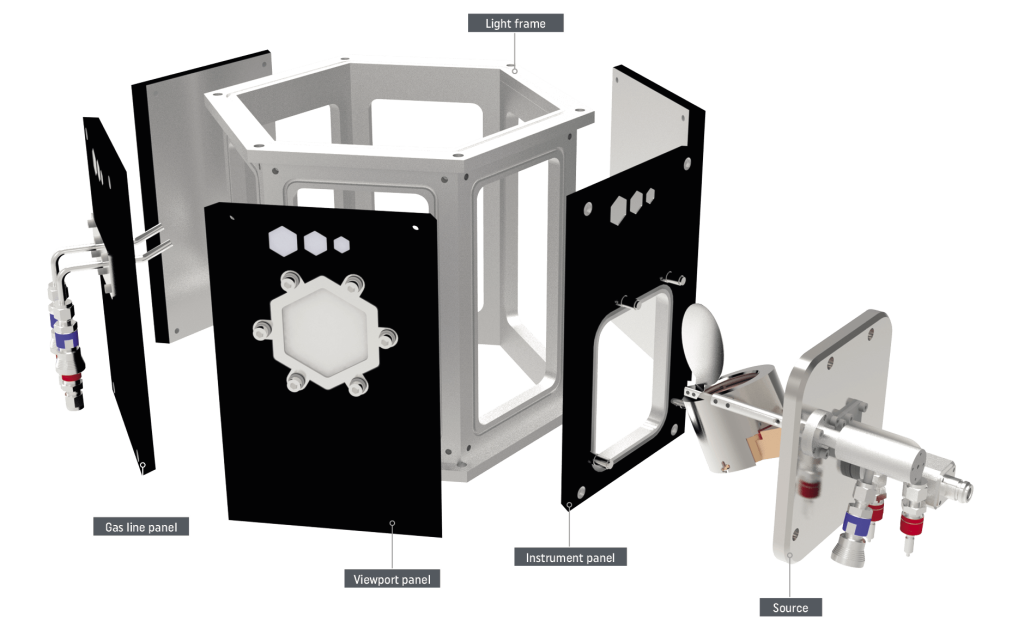
- Blank panel
- Viewport panel
- Deposition source panel
- Mass flow controller와 증착 두께 제어를 포함하는 PLD process control panel
- In-situ monitoring을 위한 QCM panel
이 디자인은 가스와 물 을 연결하기 위한 Hamlet quick connect과 샘플 스테이지 및 구성 요소 부착을 위한 개별 너트를 포함한 표준화된 피팅을 사용합니다. 이러한 표준화를 통해 간단하게 패널을 교체하고 시스템을 특정 어플리케이션에 맞게 조정할 수 있습니다. 또한 모듈식 설계로 인해 유지 관리 및 재구성이 더욱 빠르고 효율적으로 이루어집니다.
Custom Solutions for Your Requirements
당사는 증착 연구 고객의 어떠한 요구사항에도 고객사와 함께 가장 적합한 솔루션을 찾는데 협력하고 있습니다.
HEX Thin Film Deposition System APPLICATION
Designed With Research and Development in Mind
HEX 시스템은 모듈식 특성으로 인해 박막 증착 연구 개발에 이상적인 장비입니다. 모든 필수 요소에 접근성이 용이하여, 다양한 구성 요소를 테스트하고 다음을 포함한 여러 박막 증착 기술의 프로세스를 완벽하게 구현할 수 있습니다:
- 표면분석을 위한 샘플 전처리
- Sputtering
- Thermal evaporation
- 유기 PVD (Organic physical vapour deposition)
기본 모델에서 지원되는 method는 다음과 같습니다:
- 금속 및 포토레지스트 리프트-오프 공정
- EM 샘플 전처리
- 신규코팅 연구개발
- 마그네트론 스퍼터링 증착 최적화
사용 사례에 추가 기능이 필요한 경우 HEX 시스템에는 대부분의 박막 증착 프로세스에 대한 시스템 범위를 확장하는 다른 많은 모듈이 포함되어 있습니다.

THE HEX SERIES
FUTURE-PROOF
complete flexibility in your process
The HEX series offers complete flexibility in your process. Whether you need the standard, L or XL, all systems are future-proof.
Upgrade or Modify with Ease. Add sources at any point in the systems life without needing long system downtimes.
Stack it. Stack your HEX at any point in its life to optimise process parameters when longer throw distance is needed.
Sputter up or Sputter Down. Switching the detachable top or bottom plates allows either configuration, with sputter up useful for evaporative methods, while sputter down eliminates shadowing on heavier samples.
Source to Substrate Distance and Angle. Utilise the HEX series’ modularity to change source-sample distance and angle at will. This gives users complete control over their process parameters, useful for optimising uniformity, deposition angle and thermal load on the substrate.
THE HEX SERIES
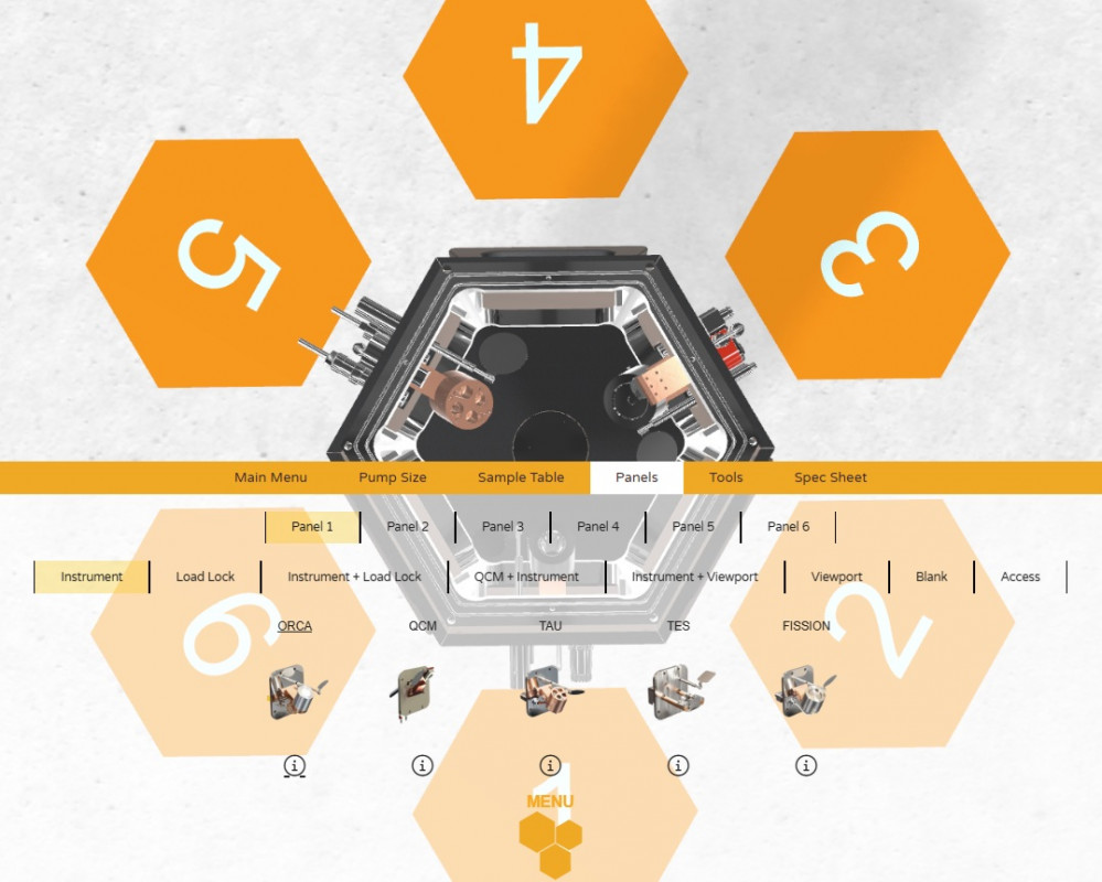
HEX Configurator
Build your Perfect PVD System
Our HEX configurator works just like a car configurator, but for scientific instruments. Select your HEX size, then customize it with sources, turbo pumps, load-locks, QCMs, and viewport panels to match your exact application requirements.
Once configured, you can explore your system from every angle, remove the chamber top to see inside, capture screenshots, review the detailed specification sheet, and even download the complete 3D model.
Please note: This is a comprehensive 3D configurator and may take a moment to load.
The HEX Thin Film Deposition System Sources
HEX 시리즈는 다양한 증착 소스의 사용이 가능합니다. 이는 사용자의 용도에 따라 복합적으로 혹은 단일 소스만으로 구축될 수 있고, HEX와 HEX-L 모델 간에 전환이 가능합니다. 견고하게 설계되고 유지 관리가 용이한 Korvus Technology의 증착 소스는 HEX 및 HEX-L PVD 시스템에 이상적인 조합을 제공합니다.
TAU E-Beam Evaporation System
ORCA Organic Evaporation System
TES Thermal Evaporation System
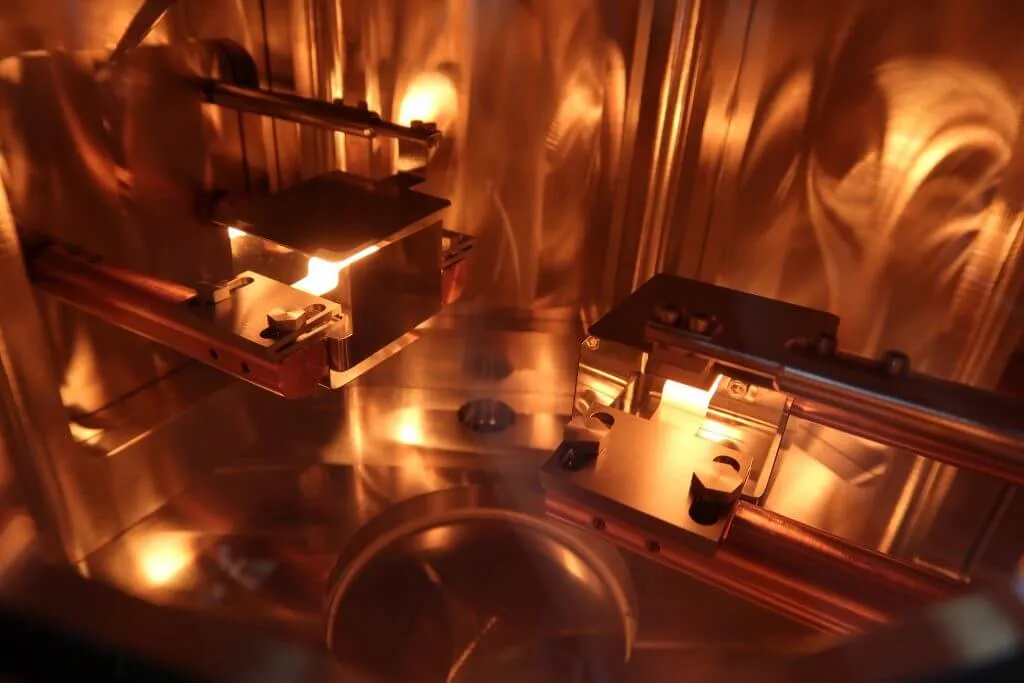
Fission DC and RF Sputtering System
Frequently Asked Questions
How Do PVD Systems Work In The Thin Film Deposition Process?
Thin film deposition refers to any technique where a very thin film of material, usually only a few atoms thick, covers a particular substrate. What makes this process attractive is the versatility and range of both the coating and target material, which allows the coating to improve or alter the substrate’s performance. Common applications include making the substrate scratch-resistant, making it more or less electrically conductive, or improving on a substrate’s durability.
The two primary methods of thin film deposition systems rely on either a physical evaporation process or chemical reactions to atomise the source material before bonding it to the substrate layer by layer. Physical processes rely on very low pressures and commonly use a resistive heat source to produce the required vapour pressure, while chemical processes use reactive gas and another precursor gas. When the two gases interact on the substrate, a chemical reaction occurs that results in an even film without the need for spin coating methods that may influence thickness or purity.
What Is a PVD System?
A PVD system is a machine designed to create thin-film coatings on a variety of materials. Operating within a vacuum chamber, it vaporises solid materials and deposits them onto a substrate. This precise deposition process can produce highly durable coatings, coatings with high electrical or thermal conductivity and coatings with many other properties, with meticulous control over thickness and composition.
The PVD process involves several stages: evaporation, transportation, condensation and bonding. There are many methods of PVD coating with their own use cases that you can read about on our website. Thermal evaporation, for example, uses high temperatures to vaporise the target material. Alternatively, sputtering employs ionised gas to bombard a target, dislodging atoms for deposition. Thermal evaporation offers higher throughput, while sputtering provides exceptional uniformity and minimal impurity levels.
PVD systems are capable of coating a wide range of materials, including metals, wafers, glass slides and more. They are widely used in industries requiring robust and durable coatings for applications in the medical, aerospace and solar industries. The vacuum environment ensures purity and strong adhesion, resulting in long-lasting, high-performance coatings.
What Are The Uses of PVD Coating?
Creating thin films with PVD coating allows manufacturers to change or enhance the properties of the substrate. The material is deposited onto the substrate in a controlled process, providing additional durability or conferring new properties such as conductivity, transparency or reflectivity.
What Are The Advantages of Using Physical Vapour Deposition Systems?
PVD systems provide precise and durable coatings for a wide range of applications. PVD is used due to the coatings’ adhesion, durability and resistance to wear.
Advantages include:
- Versatility: Coatings can be vaporised in a vacuum and deposited atom by atom, allowing for precise multilayer films.
- Efficient processes: The techniques ensure uniform coatings by precisely controlling the deposition of atoms or molecules, reducing waste and enhancing efficiency, even for complex substrates.
- Enhanced properties: The use of oxygen and other reactive gases enables compound materials (e.g., titanium nitride) for corrosion resistance and reduced friction.
- Environmentally friendly: PVD produces functional and protective coatings with no toxic residues.
What Makes the HEX Series Unique?
Many bench-top thin film deposition systems are pre-welded solid instruments that offer limited functionality. The HEX series is unique amongst thin film deposition systems due to its versatility — its modular design allows for customisation and robust user control features. Not only does this make the HEX ideal for teaching about various thin film techniques, but it also allows research and production facilities to incorporate the latest advancements in thin films into their bench-top system.