메뉴 건너뛰기

반도체 소재 측정분석 및 증착, 이온밀링, 마이크로 머시닝 솔루션

Sputtering System (진공증착장비)

미국 AJA사는 R&D 스케일의 physical vapor deposition (PVD)를 위한 마그네트론 스퍼터링 시스템 (magnetron sputtering system)을 제공합니다. 본 시스템은 con-focal 또는 normal incidence, off-axis, glancing angle, "target to substrate orientation"의 combination으로 구성할 수 있습니다.


Ion Milling System (이온 밀링 시스템)

기판 쿨링과 SIMS end point detection 기능으로 다양한 크기를 물리적으로 에칭하는 시스템입니다. 최대 22 cm 직경의 RF 이온소스와 DC 이온소스가 가능합니다. 대형 소스를 위한 편리한 슬라이드 레일 액세스.

AJA사의 ATC-IM 이온 밀링 시스템은 특정 요구 사항에 따라 다양한 구성으로 구축되는 다목적 툴입니다. 챔버는 원통형 또는 박스 스타일, HV 또는 UHV 일 수 있습니다. SIMS end point detection은 AJA의 고유 한 SIMS-IS isolation system과 함께 옵션 사항으로, 메인 챔버가 벤트될 때마다 SIMS head/detector를 진공 상태로 유지할 수 있습니다. 


Evaporation System (E-Beam 증착 및 열증착)

AJA International의 ATC-E (E-Beam Evaporation) 시스템과 ATC-T (Thermal Evaporation) 시스템은 R&D 규모의 박막 증착을 위해 설계된 고도로 진화된 HV, UHV 코팅 장비입니다. 본 시스템은 로드 락 (load-lock), 이온 밀링 / 이온 보조 소스, 가열 / 냉각 기판 홀더, QCM 증착 제어 / 컴퓨터 컨트롤, AJA의 고유한 수냉식 300 Amp 열 증착 소스를 특징으로 합니다.


Multi-Technique & Hybrid System (멀티 시스템)

ATC-M 시리즈 Multi-Technique System은 싱글 챔버 (하이브리드 시스템) 또는 멀티 챔버 (멀티 챔버 시스템)에서 다양한 박막 증착 (thin film deposition)과 이온 밀링 (ion milling), 분석 작업을 결합하여 진공상태를 유지하면서 기재 또는 기판 (substrate)의 in-situ 이송을 허용하는 "공정과 공정을 잇는 다목적 장비"입니다. 본 시스템은 HV 또는 UHV로 구성되며, 원통형 또는 박스형, 가공 챔버 스타일로 구축할 수 있습니다.

Magnetron Sputtering, E-Beam Evaporation, Thermal Evaporation, Ion Milling, Ion Beam Deposition, Pulsed Laser Deposition (PVD), Ellipsometry, Rapid Thermal Anneal, Oxygenation and Nitridization, XPS/AUGER/LEED Analysis, MBE, RHEED, MOS, SIMS, RIBE

  • Multi-Chamber Systems - with deposition, milling, evaporation, annealing, PLD, load-lock and analysis in connected chambers.
  • Hybrid Systems - load-locked single chambers with some combination of deposition, milling, evaporation, annealing, PLD and analysis.


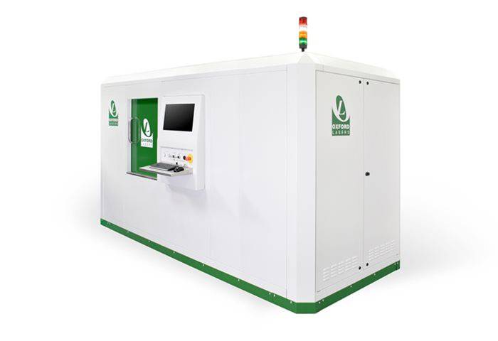
Laser Micromachining Systems 
반도체 소재 미세가공 시스템

This group of materials, with conductivities that fall between normal conductors and insulators, can be laser machined with extremely high precision irrespective of whether they fall into the class of materials that form the intrinsic or extrinsic group.

Laser micromachining can be used to process almost all semiconductors with ultra-high accuracy and precision.  This can be particularly important as devices shrink in size where tolerances become ever more demanding. Lasers not only allow drilling of hard semiconductors like Silicon Carbide and Diamond, but also micro cutting where laser kerf widths are significantly reduced compared to conventional dicing or sawing. MORE DETAILS 
 

Silicone Nitride
  • Many semiconductor materials e.g. Silicon can not only be drilled and cut but can also be trimmed and the material wafers re-sized.  Wafer resizing can routinely be achieved on wafers up to 300mm.
  • In addition, it is possible to mill or thin these semiconductor materials with degrees of precision approaching a few microns.  This can be particularly useful for creating new devices or for semiconductor analysis.


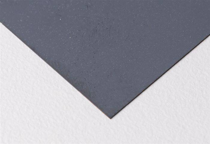
A sample of semiconductors we can machine include:

  • Gallium Arsenide | Germanium | Silicon | Silicon Carbide | plus many more...
 

유전율측정기 (Permittivity, Loss Factor, Tangent Delta)