Written by Bryan Stuart
Published on
An Introduction to Electron Beam Evaporation and E-Beam Evaporators
Electronic beam evaporation, also known as e-beam evaporation, is one of the four main forms of physical vapour deposition (PVD). It uses an intense beam of high-energy electrons to evaporate the source material [1], reducing limitations on maximum evaporation temperatures.
E-beam evaporation works in a different way to sputtering, which collides energetic ions with a target to sputter or eject the target material. Electron beam evaporation expands upon the applications of thin film deposition common to more traditional vaporisation processes.
But which method is better? Is electron beam evaporation what you need from your thin film deposition system?
Read ahead to learn the ins and outs of electron beam evaporation, along with its advantages over sputtering, from our Korvus Technology team.
The TAU E-Beam Evaporator
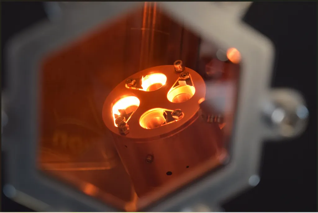
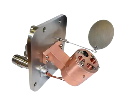
The TAU e-beam evaporator stands out with its compact framework, uniquely opting out of the use of beam-bending magnets that are common in bulkier counterparts. Instead, it leverages a positive charge to direct a focused electron beam towards a target crucible, with a DC voltage applied to a tungsten filament to initiate indirect heating and evaporation of the material.
Central to the discussion on the e-beam evaporator process is the heat management during material vaporisation. The electron beam is accelerated under controlled conditions to minimize excessive thermal build-up. The TAU incorporates an ingeniously designed enclosed head, significantly reducing the thermal footprint within the vacuum chamber. This meticulous design allows for deposition at lower substrate temperatures, making the TAU an invaluable asset for lift-off techniques and the coating of heat-sensitive substrates, ensuring precision and integrity in the final application.
The Electron Beam Evaporation Process

Electron beam evaporation is a form of physical vapour deposition that uses a focused electron beam within a vacuum environment to heat evaporation material. The e-beam evaporation process is based on the emission of electrons from a tungsten filament when exposed to a current.
The electron gun system sends an electric current of sufficient energy, between five and ten kV, through the tungsten filament, which is located outside the deposition area. This high-voltage current heats the tungsten to high temperatures, allowing the thermionic emission of electrons to occur.
The e-beam evaporator then uses permanent magnets or electromagnetic focusing to direct the high-energy electrons toward the target material, which is placed in a water-cooled crucible.
As the crucible is bombarded with an electron beam, the kinetic energy is converted into thermal energy. This causes the material inside to evaporate, rise through the vacuum chamber and deposit onto the substrate as a thin layer.
This focused, high kinetic energy can evaporate high melting point materials not capable of evaporation through traditional deposition methods. It can yield very high deposition rates at low substrate temperatures.
This method of thermal evaporation is useful for deposit metals, refractory metals, optical thin films, and a range of other electron beam evaporation applications.
The Main Advantages of Electron Beam Evaporation
Electron beam evaporation offers excellent precision and versatility. It enables the vaporisation of materials with high melting points, such as tungsten and niobium, and provides exceptional control over the coating process.
High-Temperature Thin Film Deposition
One significant advantage of electron beam heating is the ability to work with higher deposition temperatures than traditional thermal evaporation. This method of evaporation can vaporise coating material metals with high melting temperatures, such as
- Tungsten
- Niobium
- Silicon dioxide
- Ruthenium
Coating Control
Electron beam evaporation allows for high material utilisation and is applicable across a broad range of evaporation materials. Using the electron beam allows for precise control over the deposition rate and monitoring of the growing film on the substrate. Using an electron beam evaporator enables you to create a coating that matches your desired properties, down to a fraction of a nanometre.
Substrate Protection
 Processes like sputtering can cause damage to the substrate because the high-energy particles involved in the sputtering process can physically dislodge atoms from the substrate, leading to erosion or the implantation of unwanted materials. This action can also introduce thermal stresses due to the high kinetic energy of the particles impacting the substrate, potentially altering its physical and chemical properties.
Electron beam evaporation, on the other hand, minimises damage to the substrate as it utilises an electron beam to heat and evaporate the source material in a vacuum. This method allows for more precise control over the deposition rate and substrate temperature, reducing the risk of thermal damage. Additionally, since the process is less aggressive compared to sputtering, there’s a lower likelihood of substrate alteration or damage from high-energy particle impacts.
Applications
Electron beam evaporation applications vary between ceramic coating deposition [2], the growth of zinc oxide thin films [3], creating coatings to protect surfaces in corrosive environments, and more.
One of the most promising uses of electron beam evaporation is within laser optics. The thin films produced by this thermal deposition process are ideal for optical coatings, such as those on solar panels, eyeglasses, architectural glass, and more.
Electron beam evaporation is also applicable in the aerospace and automotive industries. These industries often have high temperature requirements and strict guidelines for the wear resistance of their materials.
Comparing Electron Beam With Other Thin-Film Deposition Processes
A common question is, “How do I know if I should use e-beam over deposition methods?”
The thin films deposited with different PVD techniques vary, as well as different procedures being suited to different coating materials. Take a look below to see common comparisons.
E-Beam Evaporation vs Thermal Evaporation
E-beam evaporation is used over thermal evaporation when high energy and precise control over the evaporation rate and substrate temperature are required. This method is particularly beneficial for materials that have very high melting points or those that are sensitive to thermal decomposition.
With that being said, thermal evaporation is a great choice if you are working with materials that evaporate at lower temperatures and require a simpler, more cost-effective setup. Thermal evaporation can offer a uniform and high-quality coating for a wide range of materials, making it suitable for applications where material properties allow for its use.
E-Beam Evaporation vs Sputtering
Electron beam evaporation and sputtering both have a range of applications. However, electron beam physical vapour deposition allows for the vaporisation of high-melting-point materials with a relatively low deposition time [4].
E-beam evaporation is more suitable for high-volume batch production and thin-film optical coatings. While sputtering is applicable to some optical processes, its applications are more limited. As such, sputtering is more commonly used within applications requiring high levels of automation.
FAQs About E-Beam Evaporation
How Is Sputtering Different from Electron Beam Evaporation?
While sputtering and e-beam evaporation are both forms of physical vapour deposition, their deposition processes differ significantly.
Electron beam evaporation is a form of thermal evaporation. The thermal evaporation process focuses an electron beam on a source material to produce very high temperatures, allowing it to vaporise high-temperature materials.
Meanwhile, magnetron sputtering collides positively charged energetic ions with a negatively charged target material, ejecting atoms from the target material and depositing them onto a substrate. Sputtering occurs within a closed magnetic field, while electron beam evaporation occurs within a vacuum or deposition chamber.
Both sputtering and e-beam evaporation have a low level of impurity, but e-beam PVD has a higher deposition rate. However, sputtering has the highest rate of scalability, as it can be automated in many applications.
In some cases, using ion-beam-assisted deposition, such as that involved in sputtering, can expand the functionality of thermal evaporation. Understanding the right evaporation system, or the right combination of systems is essential to optimising precision, functionality, and efficiency in your desired application.
What Are the Disadvantages of E-Beam Evaporation?
While electron beam PVD has some industrial applications, it is not suitable for coating the inner surface of complex geometries. Additionally, the filament degradation used within this vaporisation process can produce a non-uniform evaporating rate, producing less precise results than other methods.
Evaporation deposition also has limited scalability with a lower utilisation and deposition rate. Further, this system is relatively complex, leading to a higher cost compared to other deposition methods, like pulsed laser deposition or chemical vapor deposition.
Weighing up the advantages and disadvantages of this thermal evaporation technique can help you determine whether it is suitable for your application.
References
[1] Bashir, Almas, Iqbal Awan, TAhir, Tehseen, Aqsa, Bilal Tahir, Muhammad, Ijaz, Mosin. (2020, May 27). Interfaces and surfaces. Chemistry of Nanomaterials. Retrieved December 28, 2022, from https://www.sciencedirect.com/science/article/pii/B9780128189085000032
[2] Shamala, K. S., Metzner, C., Maiti, N., Zhigarev, A. A., Evans, ?., Kanareykin, A. D., Ganz, S. N., Avdeeva, D. K., Garshin, A. P., Balkevich, V. L., Kunevich, A. V., … Hocking, M. G. (2017, June 19). Ceramic coating deposition by electron beam evaporation. Surface and Coatings Technology. Retrieved December 28, 2022, from https://www.sciencedirect.com/science/article/abs/pii/S025789721730645X
[3] Caglar, M., Fang, G. J., Karuppasamy, A., Asmar, R. A., Zhu, B. L., Daniel, G. P., Fang, Z. B., Zhang, D. H., Chu, S. Y., Zhaoyang, W., Li, X. H., & Kim, D. C. (2011, March 29). Effect of heat treatment on characteristics of nanocrystalline ZnO films by electron beam evaporation. Vacuum. Retrieved December 28, 2022, from https://www.sciencedirect.com/science/article/abs/pii/S0042207X11001205[4] Maiti, N., Karmakar, P., Barve, U. D., & Bapat, A. V. (2008). An evaporation system for film deposition using electron beam sources. IOPScience. Retrieved December 28, 2022, from https://iopscience.iop.org/article/10.1088/1742-6596/114/1/012049

