

Written by Korvus Technology
Published on
Sputtering: What is it and how does sputter deposition work?
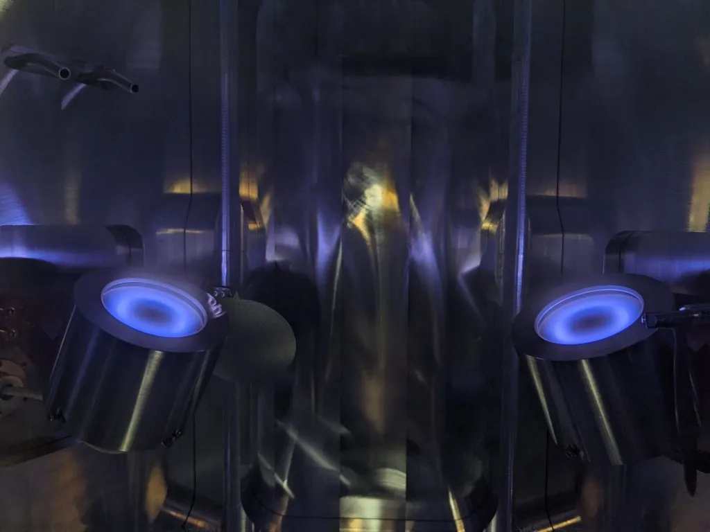
Most people are familiar with the three states of matter: solid, liquid, and gas. However, gaseous plasma exists as a state apart. This unique dynamic condition creates a flux of neutral gas atoms coexisting with electrons, photons, and accelerated ions in the same space. Since plasma consists of unstable high-energy particles (i.e., ions and electrons), it needs an external energy source like powerful voltages or high temperatures.
Gas plasma has many uses across different industries, one of which is a surface modification by sputter deposition. Physical sputtering[1] is a thin film creation method that directs accelerated ions from the source material onto a target surface to create a coating. This technique has applications in the semiconductor industry and solar panels, disk drives, optical devices, and other major industries.
This overview covers the basics of the sputter deposition method and its advantages compared to other deposition methods.
What Does Sputtering Mean?
The word “sputtering” originates from the Latin “Sputare,” which means “to spit out noisily.” You may picture a spray fountain made up of tiny moist particle flux. While crude, this image depicts the gaseous plasma-based sputter remarkably well.
People who deal with car mechanics may also associate “sputter” with the series of explosive noises an engine makes when it overheats and is about to give out. In industrial physics, however, the meaning of “sputtering” has an entirely different context.
This process is one of many forms of Physical Vapour Deposition (commonly refer as PVD). One of its most widely used alternatives is the thermal deposition method.
Sputtering is a process that enables the creation of film coating made of sputtered atoms. Without this method, it would be nearly impossible to attain the high-quality coating films necessary for LED displays, optical filters, precision optics, and more.
Plasma sputter began in 1970 [2] when Peter J. Clarke presented the first sputtering device that used electron and ion collisions to deposit an atom scale coating on a target surface. Today, more than five decades later, thin film applications form an inseparable part of aerospace, solar energy, microelectronics, automotive, and other industries.
The Sputtering Process
The sputtering process starts with placing the substrate (the surface that requires a coating) in a vacuum chamber filled with inert gas atoms.
The source material, which will transfer onto the substrate, then receives a negative charge and becomes a cathode. This causes free electrons to flow from the charged source materials. These electrons collide with the outer electrons surrounding the gas atom, which has the same negative charge, driving the gas electrons off. Once it loses electrons, a neutral atom turns into a high-energy ion.
When the cathode target is bombarded, electrons get knocked out due to the collisions, and the gas atoms turn into positively charged ions. The negatively charged source material attracts these positive ions, which fly at it with such high velocity that atomic-sized particles “sputter off,” or detach.
Finally, the sputtered particles cross the vacuum chamber and start landing on the substrate surface as a growing film made of ejected target ions.
How Does Sputtering Work?
Sputter systems come in different sizes, depending on the industry application. The process happens in a vacuum chamber. Glass (e.g., architectural glass, solar cells, and so on) is the most common substrate for the film coating.
Korvus Technology manufactures the HEX Series, a sputtering system capable of several thin film deposition techniques. The sputter coating is one of the most common applications of this incredibly versatile and efficient system.
What Is a Sputtering Target?
T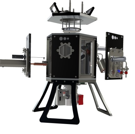 he film material source is a rotary target made of metal, ceramic, or even plastic. As an example, let’s take a molybdenum target. Molybdenum often functions in producing conductive thin films in displays or solar cells.
Throughout the process, pumps keep removing air to create a vacuum environment. The base pressure in the chamber is around 10 to -6 millibar or about a billionth part of the normal atmospheric pressure.
Inert gas atoms flow continuously into the deposition chamber, creating a low gas pressure atmosphere.
In physical vapour deposition,[3] a magnet array may sit inside the cylindrical target, releasing a magnetic field. Cooling water inside the target cylinder dissipates the heat generated in the process.
How does a sputter coater work?
Under high voltage, the molybdenum target creates a gaseous plasma, which concentrates along with the magnetic fields. The plasma consists of gas atoms, free electrons, and positively charged argon ions.
Continuous electron collisions with the argon atoms keep producing positively charged ions. Since the target surface, or the cathode, is negatively charged, its binding energy attracts the energetic ions. As the target gets bombarded, ions displace atoms. You could think of it as a billiard ball that collides with another ball and sends it rolling.
The sputtered atoms gradually settle on the glass substrate, or the anode, which sits opposite the target. Layer by layer, these ejected atoms form a thin film.
This process’ deposition rate calculation depends on various factors, such as the target material’s physical properties, the current, and beam energy.
Target Surface Quality
Ions that hit the target surface don’t distinguish between the desired target atoms (e.g., molybdenum) and any impurities with the same charge. Any atoms that get ejected may consist of both.
If the target surface contains impurities, they may end up on the substrate as sputtered atoms and compromise the thin film properties, such as its electrical conductivity. To ensure high-quality thin film, the process must use a highly pure target by a trustworthy manufacturer as well as high-performing equipment.
The Role of Argon
Argon works well in sputter systems because it is an inert gas with high-mass ions. However, the reactive method may also use a non-inert gas, such as oxygen or nitrogen. In reactive setups, gas ions recombine with the target material to produce the deposited film.
Ion Beam Sputtering
Ion beam sputtering is a thin film deposition method in which an ion source sputters a target metal or dielectric material onto a substrate. The monoenergetic and highly collimated properties of the ion beam enable precise control of film growth. The result is a highly dense, superior quality film.
DC vs RF Sputtering
DC sputtering uses a DC (Direct Current) power source. This method is widely used, effective, and economical. It allows the processing of large substrate quantities.
The RF sputtering method uses a high voltage AC (Alternating Current) power source and works for both conductive and non-conductive sputtered material. The RF stands for radiofrequency. This technique is more expensive and has a lower sputter yield, making it more suitable for lower substrate sizes.
Magnetron Sputtering
Magnetron sputtering[4] relies on magnetic fields to control the velocity and direction of charged ion particles from the magnetron sputtering source. Although diode sputtering can yield atomic-scale thin films, it is a slow process that works best with a limited-size substrate. Moreover, particle bombardment can cause overheating and damage the substrate.
In magnetron sputtering, magnets placed behind the cathode will trap electrons and prevent them from bombarding the substrate, creating faster deposition.
Benefits of Magnetron Sputter Deposition
Unlike other technologies, magnetron sputtering does not call for the source materials’ melting and evaporation. This process works for nearly all materials, regardless of melting temperature. The magnetic field technique allows the use of compounds and alloys as magnetron sputtering sources while maintaining their composition as similar as possible.
The Advantages and Applications of Sputtering Deposition
Sputter deposition can only occur when the bombarding particles have extremely high kinetic energy, which allows the creation of gas plasma. This method enables a pure and accurate atomic-level film deposition, infinitely superior to any conventional thermal energy techniques.
The energy transfer of the bombarding particles,[5] the target atom and ion relative masses, and the target atoms’ surface binding energy all control the sputter yield, which is the average number of atoms that fly off from the source material. The process yield’s outstanding precision and constant rate allow the exact programming of the sputtering coating thickness.
Compared to other deposition methods such as thermal evaporation, sputtering works well with a broader range of materials, including diverse mixtures and alloys. Its higher energy transfer produces better surface adhesion, more uniform films, and higher packing densities, even at low temperatures.
Many industries rely on high-quality thin films produced by the aforementioned deposition methods. Here are just a few examples:
- The optoelectronics industry, such as optical filters and precision optics
- Medical devices and implants
- Consumer electronics and LED displays
- Fibre lasers and semiconductor lasers
- Microscopy and microanalysis sample slides
Sputtering film deposition is a diverse field with many methods and techniques. It includes RF and DC magnetron sputtering, ion beam sputtering, reactive sputtering, and more.
Final Words
The sputtering deposition has brought innovation and superior performance to a wide array of industries. The method comprises many sub-techniques, all of which use high-energy collisions to create a thin, precise coating of material. Magnetron sputter deposition further expanded the range of applications and substrates.
The final film quality depends on several factors, including target material properties, process methodologies, and sputtering system performance.
Are you interested in learning more about sputtering? We invite you to read other blog articles from Korvus Technology, manufacturer of the innovative HEX Series of modular thin film deposition systems that use physical vapor deposition methods.
References
[1] Berg, S., et al. Fundamental understanding and modeling of reactive sputtering processes. Thin Solid Films Volume 476, Issue 2, 8 April 2005, Pages 215-230.
[2] Greene, J. E. Review Article: Tracing the recorded history of thin-film sputter deposition: From the 1800s to 2017. Journal of Vacuum Science & Technology, Volume 35, Issue 5, 10 May 2017.
[3] Rossangel, S. M. Thin film deposition with physical vapor deposition and related technologies. Journal of Vacuum Science & Technology, Volume 21, Issue 5, 17 June 2003.
[4] Safi, I. Recent aspects concerning DC reactive magnetron sputtering of thin films: A review. Surface and Coatings Technology, Vol 127, Issues 2-3, 22 May 2000, Pages 203-218.
[5] Mattox, D. M. Particle bombardment effects on thin‐film deposition: A review. Journal of Vacuum Science & Technology, Volume 7, Issue 3, 04 June 1998.